Blog 2 - Final Electrical PCB
Electrical
The final schematic for the PCB has been completed as shown below:
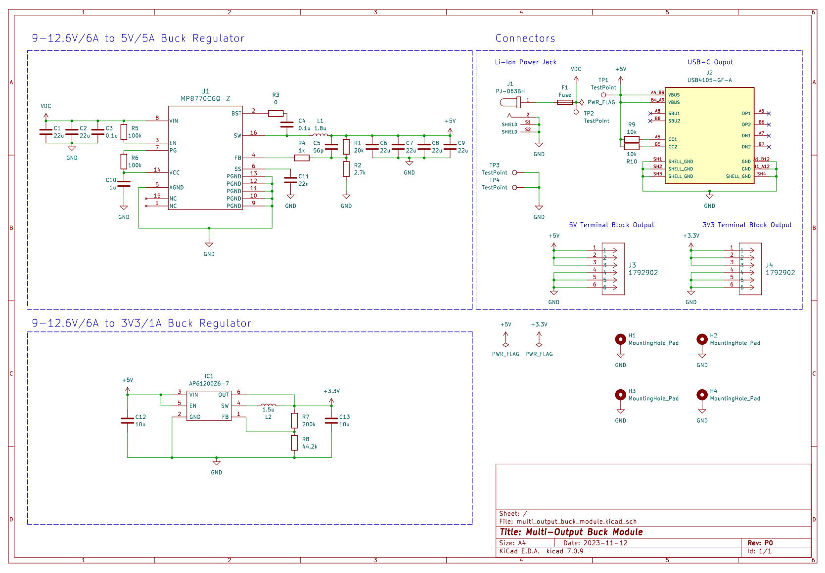
It utilizes two buck converters in two stages to step down an input voltage of 9-12.6V to 5V and then from 5V to 3V3. Our devices can then be connected and powered through USB-C or wires + terminal blocks.
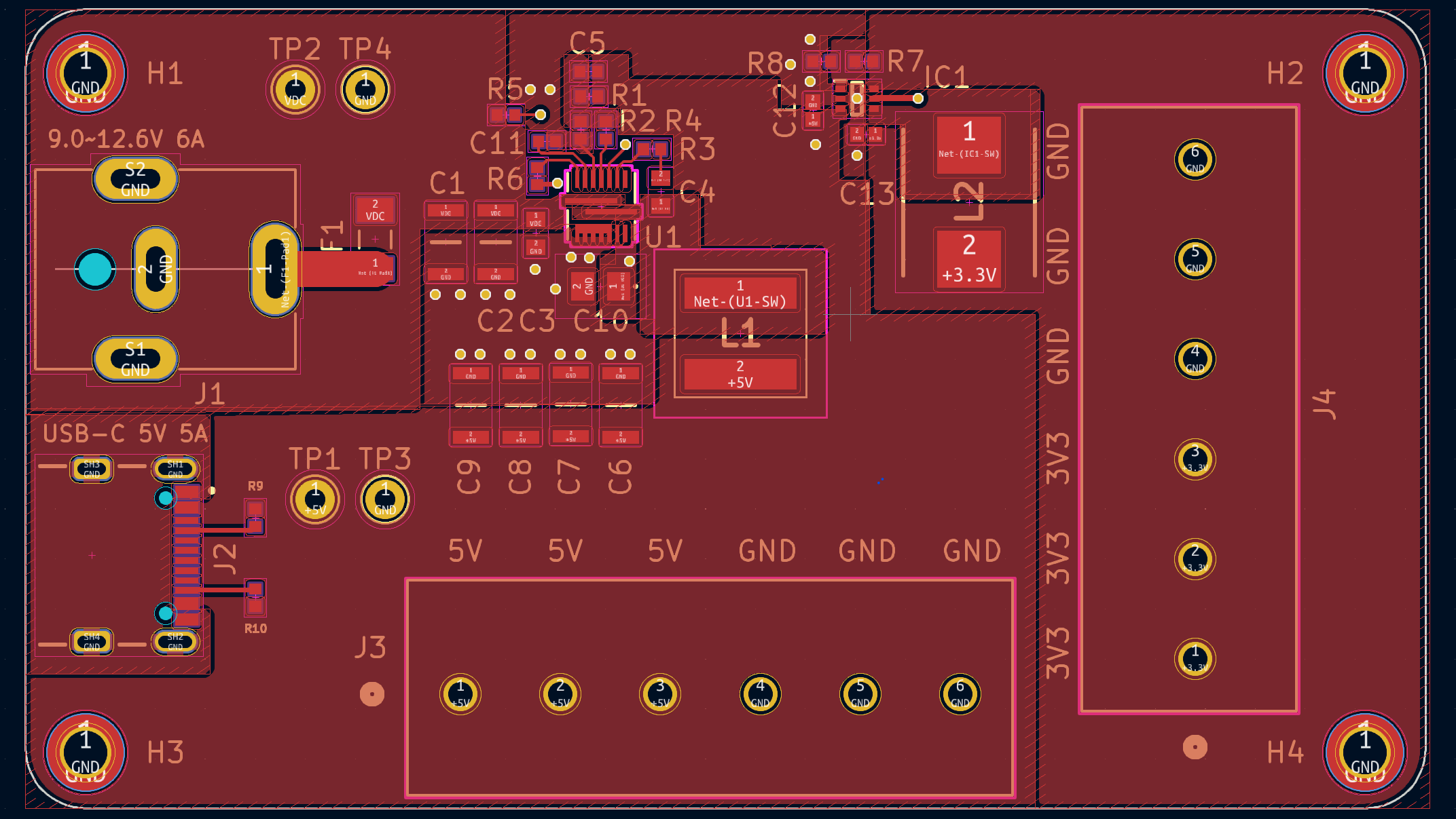
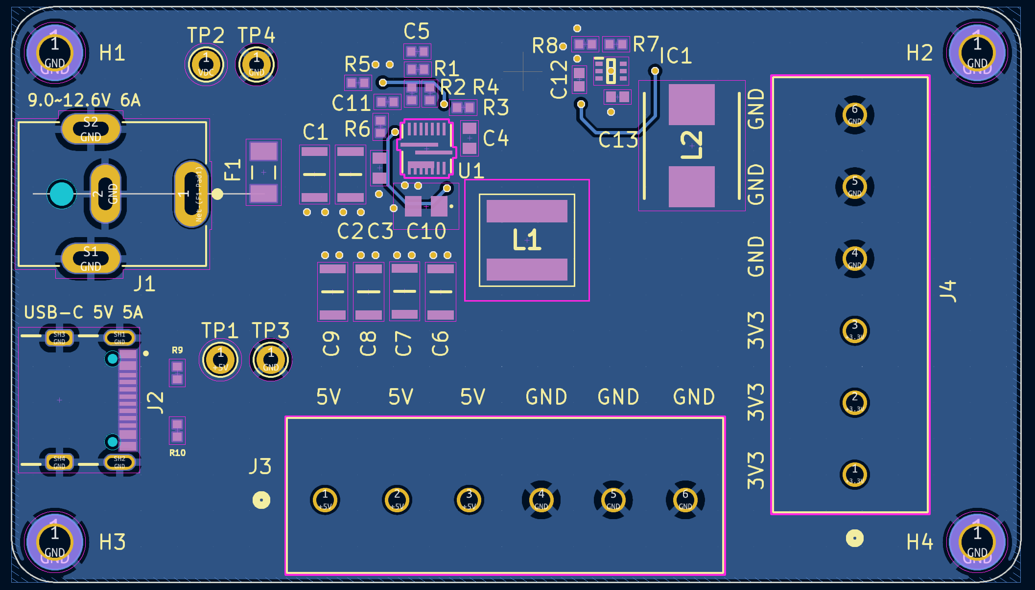
Below is a capture of the front and back copper layers of the PCB:
And an isometric view of the expected 3D model:
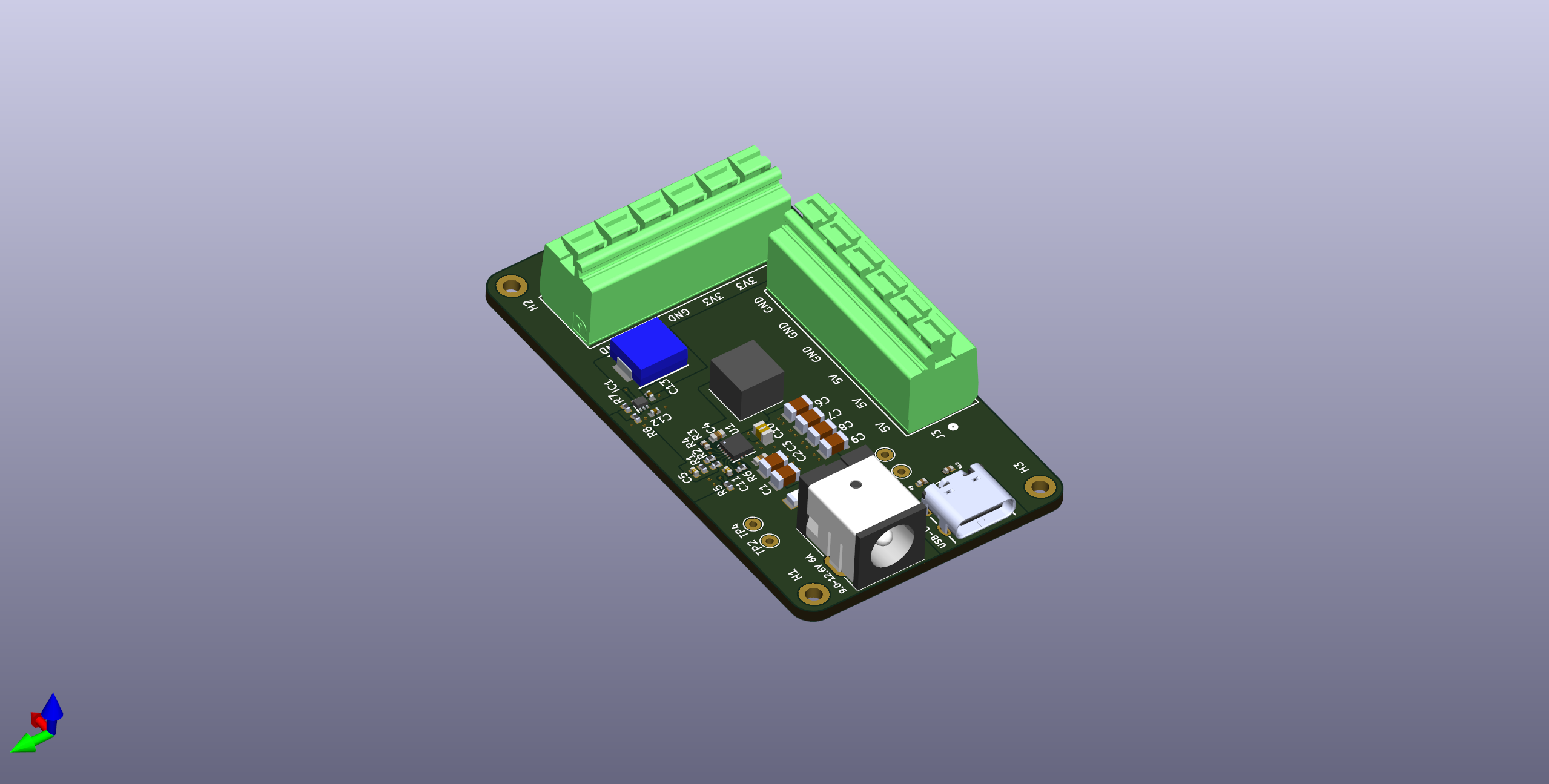
The PCB is now ready to be fabricated using PCBWay to manufacture and assemble it. The expected arrival of the PCB is around mid to late January.